IBM's sub-1 nanometer chip announcement is easy to misread. The headline sounds like a smaller transistor story. The more useful signal is that AI hardware scaling is becoming a stack design problem.
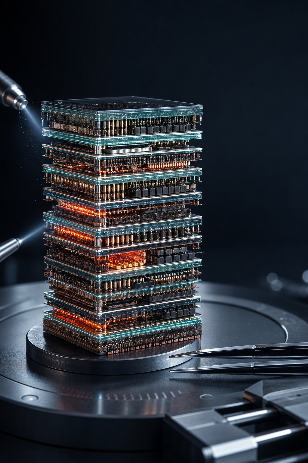
IBM says its new 0.7 nm, or 7 angstrom, node uses a three-dimensional "nanostack" architecture that can pack nearly 100 billion transistors onto a fingernail-sized chip. The company projects up to 50% more performance or 70% greater energy efficiency than its 2 nm node, plus 40% SRAM scaling.
The thesis: IBM's nanostack matters less as an immediate replacement for today's AI accelerators and more as a preview of the next AI compute constraint: how much logic and memory can be packed close together without making power, yield, and manufacturing complexity explode.
Why This Matters Now
AI infrastructure is running into multiple bottlenecks at once. More chips help, but they also demand more power, memory bandwidth, cooling, packaging, and capital. The old story was simple: shrink the node, get more performance. That story is no longer enough.
Modern node names are generation labels, not literal physical measurements. TNW correctly cautioned that "0.7 nm" should not be read as a literal feature size. Reuters also reported that IBM has not yet named a manufacturing partner for the technology. This is research-stage evidence, not a commercial GPU launch.
That distinction is the point. The useful question is not "Can buyers order this tomorrow?" They cannot. The useful question is "Which bottleneck is IBM trying to break?"
The Four-Gate Hardware Test
Use four gates to evaluate this kind of AI chip claim.
1. Architecture
IBM's nanostack shifts the conversation from two-dimensional shrinking to vertical transistor placement. Instead of only making features smaller on a flat plane, the design stacks and staggers transistors in three dimensions.
That matters because AI compute needs density, but density without usable power and thermal behavior is not enough. If 3D transistor architecture becomes practical, the advantage is not just smaller chips. It is more compute per physical footprint.
2. Memory
The most interesting number may be the 40% SRAM scaling claim. AI workloads are often limited by how quickly data can move, not just by raw math throughput. More efficient on-chip memory can reduce the penalty of constantly moving data between compute and memory.
That is why this announcement belongs in the AI infrastructure conversation. The future accelerator race is not only about more operations per second. It is about keeping the right data close enough to compute that those operations can actually be used.
3. Manufacturability
IBM says production adoption could begin as early as the next five years. That is a roadmap claim, not proof of volume economics.
Operators should separate three things: a validated structure, a manufacturable process, and a profitable product. IBM says it has shown functional CMOS inverter operation and supporting VLSI research. That is meaningful. It still leaves open yield, cost, partner selection, packaging, thermal limits, and supply-chain readiness.
This is where chip roadmaps often become strategy theater. A node can be technically impressive and still arrive too late, too expensive, or too specialized for broad AI deployment.
4. Workload Economics
IBM Research estimated that a 7 angstrom accelerator could reach about 7,000 TOPS versus roughly 1,500 TOPS for today's popular AI accelerators. Treat that as a directional estimate, not a buying metric.
For AI operators, the real metric is cost per completed workload. Training, inference, retrieval, simulation, robotics, and edge AI stress different parts of the stack. A denser chip only changes the business if it improves the full system: silicon, memory, interconnect, power, cooling, software, and utilization.
What Founders And Operators Should Do
Track the shift, not the headline.
If future AI chips are increasingly shaped by 3D integration and memory proximity, product teams should expect hardware diversity to increase. Some workloads will favor massive training clusters. Others will favor inference chips with better energy efficiency. Edge devices and robotics may care more about power per task than peak throughput.
The practical move is to build hardware-aware software without hard-coding one hardware future. Measure latency, energy cost, memory pressure, and failure modes by workload. Keep model-serving layers portable. Avoid assuming that the next generation of AI compute will simply be today's GPU pattern with smaller transistors.
IBM's nanostack announcement is not proof that AI compute scarcity is solved. It is evidence that the scaling playbook is changing.
The next AI hardware advantage may come from going up, not just going smaller.
Sources
- https://newsroom.ibm.com/2026-06-25-ibm-debuts-worlds-first-sub-1-nanometer-chip-technology
- https://research.ibm.com/blog/sub-1nm-node-chips
- https://m.economictimes.com/tech/artificial-intelligence/ibm-unveils-tech-for-chip-smaller-than-1-nanometer-in-ai-computing-push/amp_articleshow/131990596.cms
- https://thenextweb.com/news/ibm-sub-1-nanometer-chip-nanostack